
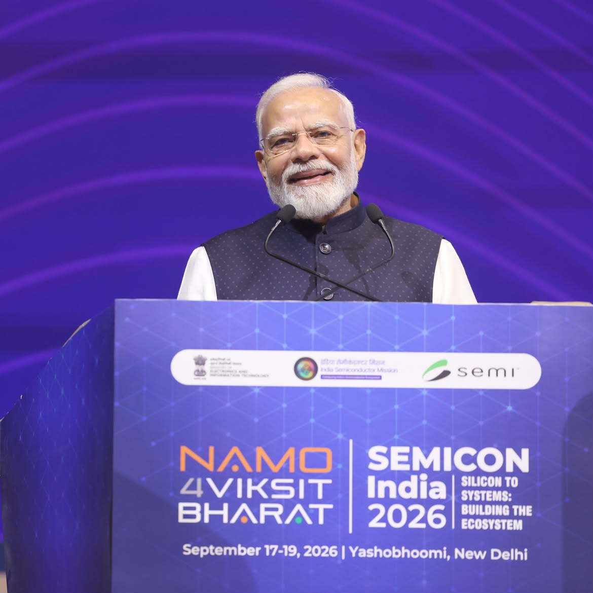
Published: September 18, 2026
Event: SEMICON India 2026
Location: Yashobhoomi, New Delhi
Theme: Silicon to Systems: Building the Ecosystem
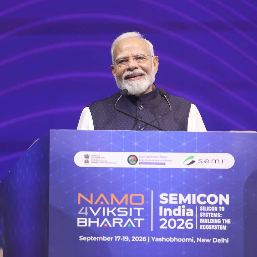
Introduction
The first day of SEMICON India 2026 highlighted India’s growing semiconductor ecosystem and its transition from policy and investment toward real-world execution. The event brought together semiconductor companies, technology leaders, policymakers, startups, researchers, equipment manufacturers and engineering talent.
Day 1 focused on semiconductor design, manufacturing, advanced packaging, AI-enabled chip development, supply-chain localization, R&D and workforce development.
Key Highlights of SEMICON India 2026 Day 1
1. India Enters the Semicon 2.0 Phase
SEMICON India 2026 highlighted the next phase of India’s semiconductor strategy, covering six major areas:
- Semiconductor Design
- Equipment & Materials
- Semiconductor Fabs
- Advanced Packaging
- Applied R&D
- Talent Development
The broader semiconductor ecosystem now connects architecture, RTL design, verification, synthesis, physical design, signoff, fabrication, packaging, testing and system integration.
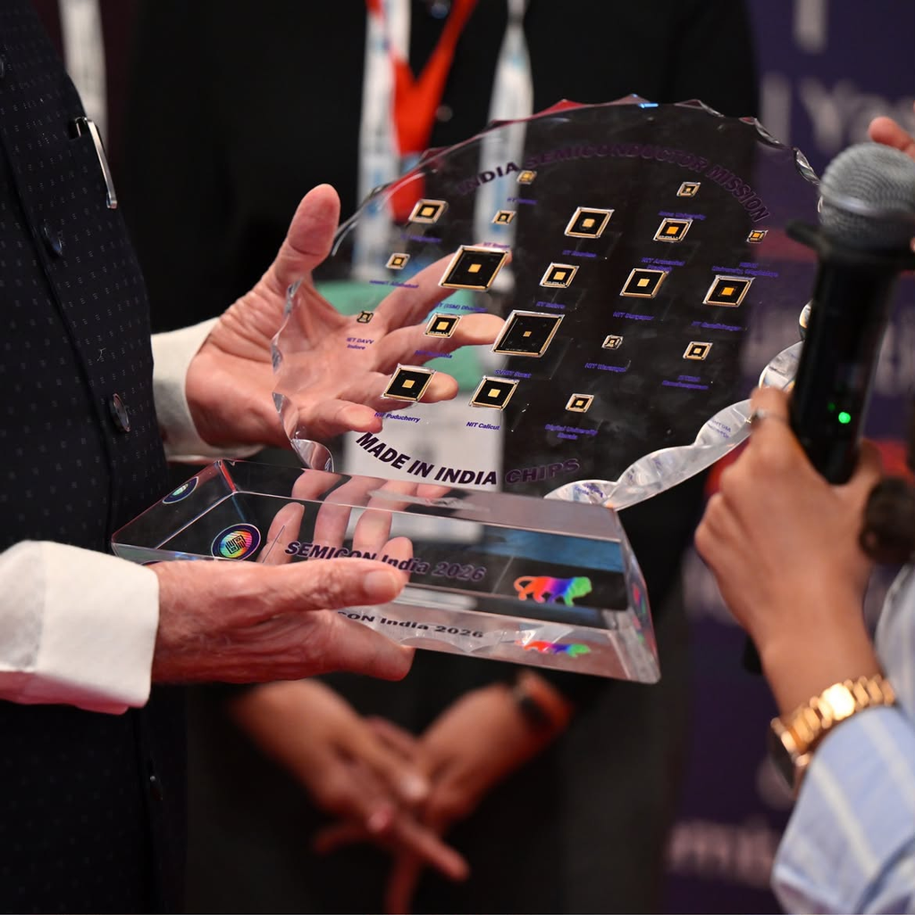
2. Semiconductor Manufacturing Moves Toward Commercial Production
Day 1 featured the virtual inauguration of commercial semiconductor production lines at CDIL Semiconductor in Mohali and Suchi Semicon in Surat.
These developments demonstrate India’s movement from semiconductor policy and infrastructure toward actual manufacturing and commercial production.
3. Major Industry Investments in India
Applied Materials announced plans for approximately US$5 billion investment in India over the next decade under its India Vision 2035 initiative.
These developments underline the importance of combining semiconductor infrastructure with skilled engineering talent.
4. Tata Electronics Strengthens the Semiconductor Ecosystem
Tata Electronics highlighted progress in its 300mm fab in Dholera and OSAT facility in Assam, along with collaborations covering wafer manufacturing, semiconductor assembly and testing, advanced packaging, materials and talent development.
5. Advanced Packaging Gains Importance
This growth creates opportunities across physical design, package design, signal integrity, power integrity, thermal analysis and verification.
6. AI Is Transforming VLSI and Semiconductor Engineering
AI-enabled approaches are increasingly being explored across:
- RTL and logic optimization
- Floorplanning and placement
- Routing and timing optimization
- Power optimization
- Test generation and coverage analysis
- Verification and debugging
- Yield analysis and defect detection
The combination of AI + EDA + VLSI engineering is becoming an important area for future semiconductor professionals.
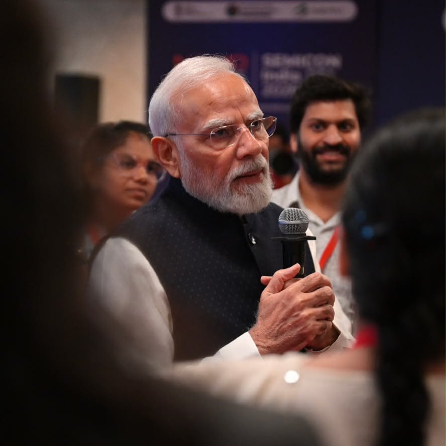
Growing Demand for VLSI and Semiconductor Talent
RTL Design: Verilog, SystemVerilog, SoC and IP Design
Verification: UVM, Functional Verification, Formal Verification and Emulation
Physical Design: Floorplanning, Placement, CTS, Routing, STA and Timing Closure
DFT: Scan, ATPG, MBIST, LBIST, JTAG and DFT Verification
Manufacturing: Process Engineering, Equipment Engineering, Yield Engineering and Process Integration.
What SEMICON India 2026 Means for VLSI Engineers
The semiconductor opportunity in India is expanding beyond traditional chip design toward a broader design-to-manufacturing and chip-to-system value chain.
The journey now connects:
Architecture → RTL → Verification → Synthesis → Physical Design → Signoff → Fabrication → Packaging → Testing → System Applications
This creates opportunities for engineers specializing in RTL Design, Verification, Physical Design, DFT, STA and Semiconductor IP Development.
VLSI Monks Perspective
At VLSI Monks, we believe skilled semiconductor engineering talent will play an essential role in India’s semiconductor growth.
As India’s ecosystem expands, engineers with practical expertise in RTL Design, Verification, Physical Design, Timing Closure, DFT and semiconductor implementation will be increasingly important.
Conclusion
SEMICON India 2026 Day 1 showcased India’s growing capabilities across semiconductor design, manufacturing, advanced packaging, equipment, R&D, supply chains and talent development.
The key message is clear: India’s semiconductor ecosystem is moving from ambition and infrastructure toward execution, production and deeper global integration.
Build Your Semiconductor Future with VLSI Monks
Looking to strengthen your expertise in VLSI Design, RTL Design, Verification, Physical Design, DFT or semiconductor engineering?
Connect with VLSI Monks to explore industry-focused semiconductor engineering solutions, training and career opportunities.
VLSI Monks – Building Semiconductor Engineering Excellence for India’s Growing Chip Ecosystem.
Frequently Asked Questions
SEMICON India 2026 is a major semiconductor conference and exhibition being held at Yashobhoomi, New Delhi, from September 17–19, 2026, under the theme “Silicon to Systems: Building the Ecosystem.”
Major highlights included the transition toward Semicon 2.0, new commercial semiconductor production lines, major investment announcements, Tata Electronics partnerships, advanced packaging, semiconductor equipment, supply-chain development, AI-enabled semiconductor technologies and workforce development.
The event highlights the expansion of India’s semiconductor ecosystem across chip design, verification, physical design, manufacturing, advanced packaging, equipment, R&D and talent development. This broad ecosystem can create opportunities for engineers with specialized semiconductor and VLSI skills.
Semicon 2.0 expands India’s semiconductor ecosystem strategy across six pillars: Design, Equipment & Materials, Fabs, Advanced Packaging, Applied R&D and Talent.