
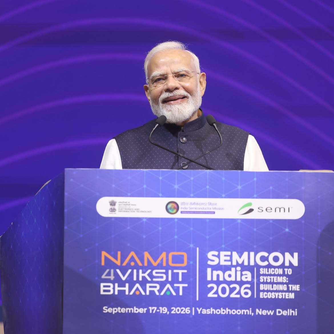
SEMICON India 2026 continued its momentum on Day 2, September 18, 2026, at Yashobhoomi, New Delhi, with a strong focus on semiconductor manufacturing, chip design, advanced packaging, supply-chain resilience, R&D, materials, talent and international collaboration.
The event, themed “Silicon to Systems: Building the Ecosystem,” brought together semiconductor companies, policymakers, technology leaders, startups, researchers, academia and engineering professionals.
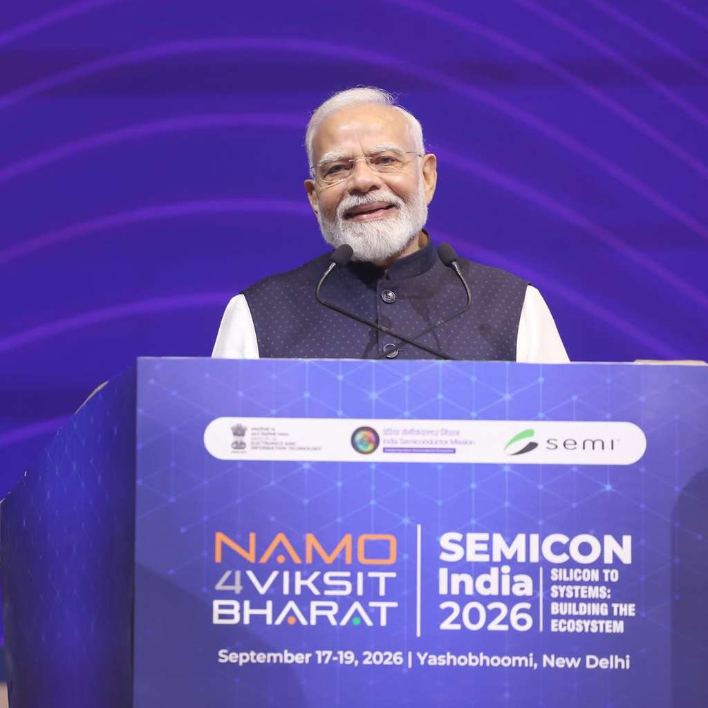
25 Major Semiconductor Announcements and Collaborations
One of the major highlights of Day 2 was the announcement of 25 MoUs, partnerships and strategic collaborations covering multiple areas of the semiconductor ecosystem.
These initiatives included:
- Semiconductor manufacturing
- Semiconductor materials
- Chip design
- Advanced packaging
- Power electronics
- Logistics
- R&D
- Supply-chain development
- Workforce and skill development
The breadth of these collaborations demonstrates that semiconductor growth is not limited to fabrication alone. Building a competitive ecosystem requires capabilities across design, IP, EDA, manufacturing, packaging, testing, materials, equipment, logistics and talent.
ISM 2.0: A Stronger Focus on Semiconductor Execution
Chip Design Emerges as a Critical Opportunity for India
India already has a large engineering talent base supporting global semiconductor companies. The next opportunity is to expand this capability toward indigenous semiconductor IP, SoC development, ASIC design, verification, physical design and product-oriented chip development.
- RTL Design
- Design Verification
- Physical Design
- DFT
- STA
- Analog and Mixed-Signal Design
- Semiconductor IP
- SoC Design
- ASIC Design
- FPGA Development
EDA and Design Automation
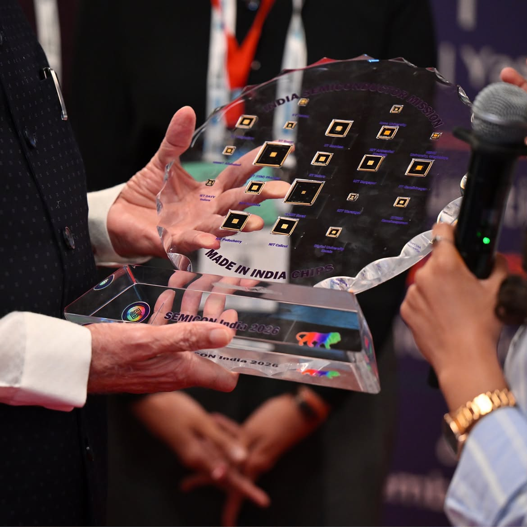
Advanced Packaging and Chiplets Gain Importance
These technologies are becoming increasingly important as semiconductor companies look beyond traditional scaling approaches to improve performance, power efficiency and system integration.
Chip Design → Physical Design → DFT → Packaging → Testing → System Integration
This makes collaboration between design, manufacturing and packaging teams increasingly important.
India–Europe and India–South Korea Semiconductor Cooperation
The India–Europe Country Roundtable brought together 139 participants and focused on investment, semiconductor equipment, materials, manufacturing, advanced packaging, chip design, R&D and talent.
The India–South Korea Country Roundtable, with 115 participants, explored cooperation across manufacturing, technology, materials, packaging, investment and supply chains.
These discussions reflect the increasingly global nature of semiconductor development, where no single region operates independently across the entire supply chain.
From Semiconductor Policy to Commercial Production
A notable theme surrounding Day 2 was India’s transition from announcing semiconductor projects to seeing projects move toward commercial production.
It requires:
Design + IP + EDA + Materials + Equipment + Fabrication + Packaging + Testing + Logistics + Skilled Workforce
The development of these interconnected capabilities can strengthen India’s position within the global semiconductor supply chain.
What Day 2 Means for VLSI Engineers and Freshers
For students, freshers and experienced VLSI professionals, the developments discussed at SEMICON India 2026 provide an important industry perspective.
RTL Design → Verification → Synthesis → Physical Design → DFT → STA → Packaging → Testing
Engineers who understand the complete ASIC/SoC design flow can better understand how individual design stages contribute to final silicon.
- Verilog and SystemVerilog
- RTL Design
- UVM and Functional Verification
- Synthesis and Lint
- CDC
- Static Timing Analysis
- Floorplanning and Placement
- Clock Tree Synthesis
- Routing
- Physical Verification
- DFT and ATPG
- Linux and scripting
- EDA tools
- Semiconductor design methodologies
A Stronger “Silicon to Systems” Ecosystem
The central message from Day 2 can be understood through the event’s theme: “Silicon to Systems: Building the Ecosystem.”
India’s semiconductor opportunity is not simply about manufacturing chips. It is about creating an integrated ecosystem capable of taking ideas from concept and architecture to design, silicon, packaging, testing and end products.
SEMICON India’s official Day 2 agenda included sessions focused on moving from concept to chip delivery and strengthening India’s design enablement and test ecosystem.
What SEMICON India 2026 Day 2 Signals for India’s Semiconductor Future
Day 2 demonstrated several important trends:
1. Indigenous chip design is gaining strategic importance.
India’s engineering ecosystem provides a foundation for developing semiconductor IP and product-oriented chip design capabilities.
2. Advanced packaging is becoming a major technology opportunity.
Chiplets, 2.5D/3D integration and heterogeneous integration are creating new engineering possibilities.
3. International partnerships remain critical.
India’s semiconductor ecosystem is developing through cooperation with global technology and manufacturing ecosystems.
4. Skilled VLSI talent will remain essential.
Building semiconductor products requires engineers across RTL, verification, physical design, DFT, testing and system engineering.
VLSI Monks Perspective
At VLSI Monks, we see the developments at SEMICON India 2026 as a reflection of the rapidly evolving semiconductor engineering landscape in India.
The growth of semiconductor design, manufacturing and advanced packaging will require engineers who can work across increasingly complex ASIC, SoC and VLSI design flows.
As India moves toward a stronger “Silicon to Systems” ecosystem, practical VLSI engineering knowledge, industry-oriented training, design methodologies and hands-on experience will become increasingly valuable for the next generation of semiconductor professionals.
Conclusion
SEMICON India 2026 Day 2 highlighted a significant stage in India’s semiconductor journey: the ecosystem is increasingly focused on converting ambition into execution.
With 25 major announcements and collaborations, stronger international partnerships, greater emphasis on indigenous chip design, advanced packaging, manufacturing, R&D and workforce development, Day 2 demonstrated the breadth of India’s semiconductor opportunity.
For India’s VLSI engineers, semiconductor startups, design companies and technology ecosystem, the message is clear: the future of semiconductor development will depend on connecting design, engineering, manufacturing, packaging, testing and systems into one integrated ecosystem.