
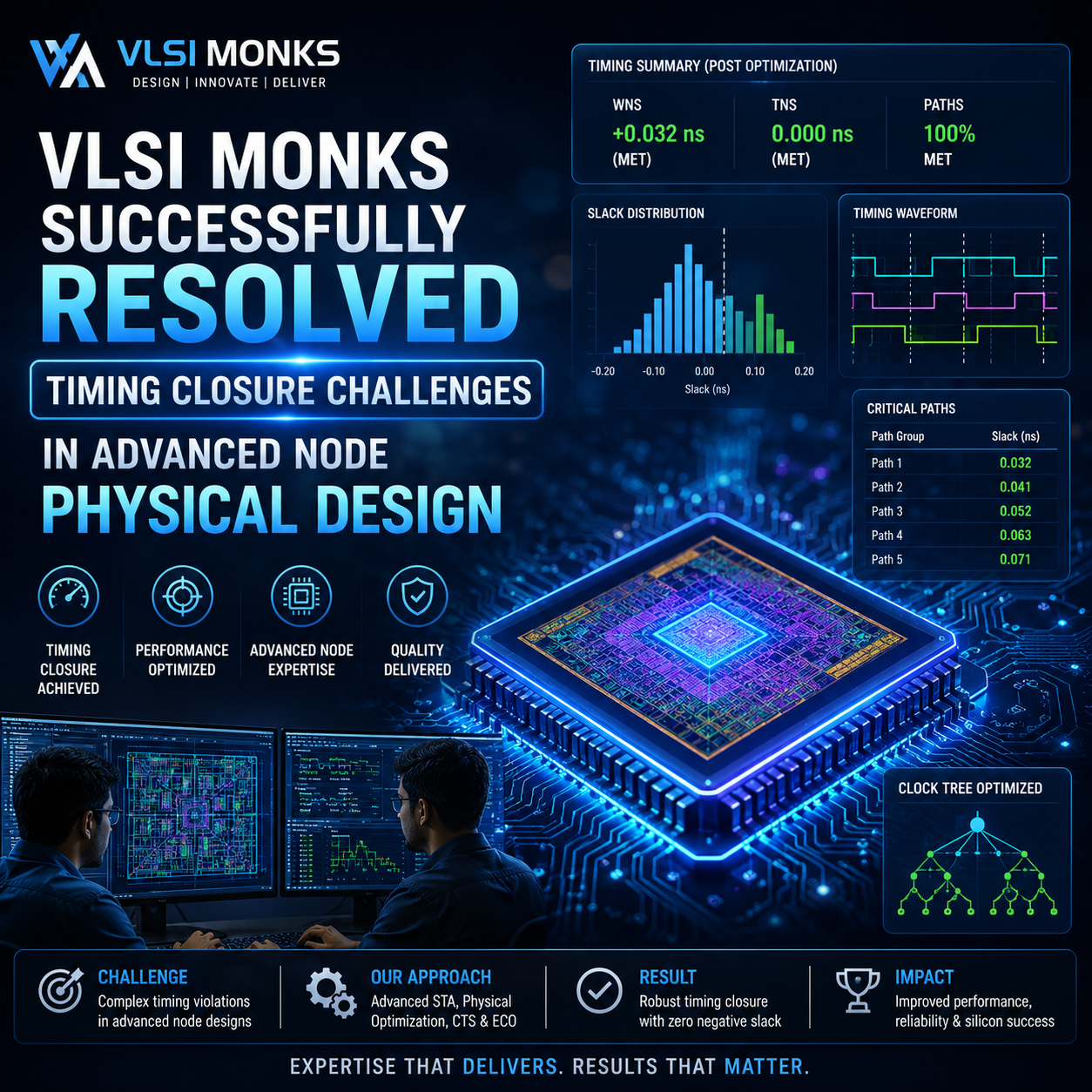
How VLSI Monks Successfully Resolved Timing Closure Challenges in Advanced Node Physical Design
Achieving Timing Closure in Advanced ASIC Designs with VLSI Monks
In today’s fast-evolving semiconductor industry, achieving timing closure is one of the most critical and challenging aspects of the VLSI physical design flow.
At VLSI Monks, a leading VLSI Physical Design Company in Bangalore, our engineering team recently partnered with a semiconductor client facing severe timing violations in a high-performance ASIC design.
Client Challenge
The client was developing a next-generation SoC targeting high-speed data processing applications :
- Multiple setup and hold timing violations.
- Excessive clock skew after Clock Tree Synthesis (CTS).
- Congestion hotspots impacting critical timing paths.
- Increased signal transition and capacitance violations.
- Difficulty achieving sign-off closure within the project schedule.
The client required expert support in Static Timing Analysis (STA) and physical design optimization to meet aggressive tape-out deadlines.
Project Specifications
| Parameter | Details |
| Technology Node | 7nm FinFET |
| Design Type | High-Performance ASIC |
| Service Offered | Physical Design & Timing Closure |
| EDA Tools Used | Synopsys ICC2, PrimeTime, StarRC |
| Methodology | Advanced Timing Optimization Flow |
Challenges Identified by VLSI Monks
After conducting comprehensive STA analysis, our team identified several root causes:
1. Long Critical Paths
Multiple timing paths exceeded the target clock period due to deep combinational logic.
2. Routing Congestion
Severe congestion in specific regions caused detoured routing, increasing wire delays.
3. Clock Network Imbalance
Non-uniform clock distribution resulted in excessive skew and uncertainty.
4. High Fan-Out Nets
Certain control signals exhibited excessive fan-out, degrading timing performance.
5. Crosstalk-Induced Delays
Signal integrity issues caused additional delay variations on critical nets.
VLSI Monks Solution Approach
Our experienced ASIC Physical Design Engineers implemented a structured timing closure methodology.
Critical Path Optimization
The engineering team performed:
- Logic restructuring and path balancing.
- Cell upsizing on timing-critical paths.
- Buffer insertion for delay reduction.
- Multi-VT optimization to improve performance.
Congestion Reduction Techniques
To address routing congestion, the team:
- Refined floorplanning strategies.
- Optimized macro placement.
- Introduced placement blockages.
- Performed congestion-driven placement optimization.
This improved routing efficiency and minimized wire delays.
Clock Tree Synthesis (CTS) Optimization
During CTS optimization, our engineers:
- Balanced clock latency across all domains.
- Reduced clock skew through buffer optimization.
- Optimized insertion delays.
- Fine-tuned useful skew methodologies.
Hold Timing Fixes
For hold violations, VLSI Monks implemented:
- Delay buffer insertion.
- Cell downsizing in non-critical paths.
- Route optimization techniques.
- ECO-based timing fixes.
All hold violations were eliminated without impacting setup timing.
Sign-Off STA and SI Closure
The final sign-off process included:
- Multi-mode Multi-corner (MMMC) analysis.
- Crosstalk analysis and noise fixing.
- OCV/AOCV timing verification.
- Signal integrity and electromigration checks.
Comprehensive sign-off verification ensured tape-out readiness.
Why Semiconductor Companies Choose VLSI Monks
VLSI Monks is a trusted provider of:
- Physical Design Services
- Design Verification Services
- ASIC Design Services
- RTL Design Services
- Layout Design Services
- Semiconductor Consulting Services
Our highly experienced engineers specialize in advanced-node design implementation, timing closure, STA analysis, and sign-off methodologies across multiple technology nodes.
Conclusion
Achieving timing closure in advanced semiconductor designs requires deep expertise, robust methodologies, and extensive experience with modern EDA tools. Through systematic analysis and optimization, VLSI Monks successfully resolved complex timing challenges and enabled timely project completion.
If your organization is facing challenges in timing closure, physical design, or ASIC implementation, VLSI Monks can help accelerate your path to successful silicon.
Partner with VLSI Monks for world-class Semiconductor Design Services and ensure first-pass silicon success.