VLSI Monks Final White Logo
  • Home
  • About Us
  • Services
    • Physical Design
    • Frontend Verification
    • RTL Design
    • Embedded Design
    • Layout Design
  • Career
  • Insights
    • Blog
    • Case Study
    • News
  • Contact
  • Home
  • About Us
  • Services
    • Physical Design
    • Frontend Verification
    • RTL Design
    • Embedded Design
    • Layout Design
  • Career
  • Insights
    • Blog
    • Case Study
    • News
  • Contact

Layout Design

Precision Crafting for High-Performance ICs

At VLSI Monks, Layout Design is more than just drawing shapes on silicon — it’s the art and science of translating circuit schematics into real, manufacturable  physical structures that deliver optimal performance, power efficiency, and area utilization.

In the rapidly evolving world of semiconductor design, achieving excellence at the layout stage is critical. Our expert team brings deep domain knowledge and hands-on experience across process nodes and foundry technologies, enabling world-class layout solutions for modern System-on-Chip (SoC) and IP designs.

What Is Layout Design?

Layout Design in VLSI is the meticulous process of positioning and interconnecting all transistor-level components of your design within the constraints of a given technology node. It bridges the gap between the logical circuit representation and the final mask data used for fabrication.

This includes:

  • Transistor placement & geometry
  • Interconnect routing across multiple metal layers
  • Power and ground planning
  • Design rule compliance (DRC/LVS)
  • Optimization for performance, power, and area (PPA)

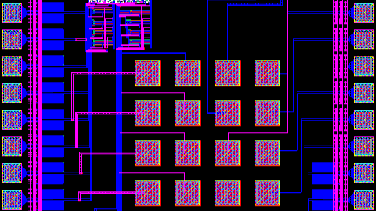
Why Accurate Layout Matters

A superior layout ensures that your IC not only meets functional correctness, but also achieves competitive performance and manufacturability:

  • Enhanced performance: Proper placement and routing reduce delays and improve timing behavior.
  • Power efficiency: Optimized power distribution and reduced parasitics help lower power consumption.
  • Reduced area: Efficient use of silicon minimizes cost and boosts yield.
  • Manufacturing Reliability: Strict adherence to design rules and verification prevents costly fabrication errors.

Our Layout Design Expertise

At VLSI Monks, we provide comprehensive layout design services across all levels of complexity — from individual transistor layouts to full-chip integration.

Transistor-Level Layout

Fine-grain placement and interconnect design for analog and mixed-signal blocks.

Block & IP Level Layout

Modular, reusable layout solutions for standard cells, memories, and custom IPs.

Full Chip Layout Integration

Complete layout assembly and verification tailored for complex SoC designs.

Multi-Node Process Support

Expertise with both advanced FinFET nodes (e.g., 5nm, 7nm, 10nm) and planar geometries (e.g., 65nm, 130nm).

Our team works with leading foundry PDKs from partners including TSMC, Samsung, UMC, GlobalFoundries, and Intel to ensure your design meets every technical specification.

Our Approach to Layout Excellence

Technology & Requirement Analysis

Understanding design goals, constraints, and target process rules.

Optimized Geometry Planning

Strategic placement and routing to balance performance and manufacturability.

Design Rule Compliance

Automated and manual checks including DRC/LVS for error-free layouts.

PPA Optimization

Iterative refinement for power, performance, and area targets.

Final Sign-Off Preparation

Integration, verification, and delivery of ready-for-fabrication layout data.

Partner With VLSI Monks for World-Class Layout Design

Whether you’re building breakthrough SoCs, high-speed IP blocks, or analog/mixed-signal circuits, our layout design services ensure your silicon meets the demands of performance, power, and precision.

👉 Let’s transform your design vision into silicon reality.

important things you should know

Questions and Answers

what is your success rate?

Lorem ipsum dolor sit amet, conse ctetur adipiscing elit. Ut elit tellus off, luctus nec ullamc orper mattis, pvinar dapibus leo.

Can you help me win?

Lorem ipsum dolor sit amet, conse ctetur adipiscing elit. Ut elit tellus off, luctus nec ullamc orper mattis, pvinar dapibus leo.

what can i expect in the process?

Lorem ipsum dolor sit amet, conse ctetur adipiscing elit. Ut elit tellus off, luctus nec ullamc orper mattis, pvinar dapibus leo.

do you provide pro bono services?

Lorem ipsum dolor sit amet, conse ctetur adipiscing elit. Ut elit tellus off, luctus nec ullamc orper mattis, pvinar dapibus leo.

can i contact you at anytime?

Lorem ipsum dolor sit amet, conse ctetur adipiscing elit. Ut elit tellus off, luctus nec ullamc orper mattis, pvinar dapibus leo.

"i'm feeling lost" - can you help me?

Lorem ipsum dolor sit amet, conse ctetur adipiscing elit. Ut elit tellus off, luctus nec ullamc orper mattis, pvinar dapibus leo.

are you looking for new attorneys?

Lorem ipsum dolor sit amet, conse ctetur adipiscing elit. Ut elit tellus off, luctus nec ullamc orper mattis, pvinar dapibus leo.

what is the best solution for me?

Lorem ipsum dolor sit amet, conse ctetur adipiscing elit. Ut elit tellus off, luctus nec ullamc orper mattis, pvinar dapibus leo.

vlsimonks

VLSIMONKS DESIGN is a fabless semiconductor company, Our main focus on R&D and design IPs.

Quick Menu

  • Home
  • About Us
  • Services
  • Career
  • Insights
  • Contact Us

Services

  • Physical Design
  • Frontend Verification
  • RTL Design
  • Embedded Design
  • Layout Design

Insights

  • Blog
  • Case Study
  • News

Contact Us

  • info@vlsimonks.com
  • +91-9538753482
  • 1st Floor, Khatta No:42/2-3, Gulmohar Enclave Rd, Silver Springs Layout, Marathahalli, Bengaluru, Karnataka 560037
Linkedin Twitter Youtube Instagram

© All rights reserved VLSIMONKS

Privacy Policy
Made with ❤ by VLSI MONKS

  • →
  • WhatsApp
  • Phone